# Security Implementation
# Protection of Flags
# Region Lock
# Description
Play a song from a region that the player is not provisioned for.
# Requirement
Confidentiality
# Protection
We verify the regions a song can be played in on every play to ensure it stays in it's provisioned regions.
# Unauthorized Play
# Description
Play a song that your user does not have access to.
# Requirement
Confidentiality/Authentication
# Protection
We check if the user is an owner or if they have had the song shared with them, and if the player is authorized to play that song based off of region provisioning information.
Additionally . . .
# Pin Extraction
# Description
Obtain the pin for a user that you do not have access to.
# Requirement
Authentication
# Protection
We hash the pins using the cryptographically secure Argon2 algorithm.
# Music Tamper
# Description
Modify a protected song. Deliver a file of the modified, protected song.
# Requirement
Integrity
# Protection
We use a digital signature to verify the music has not been tampered with.
# Custom Music
# Description
Protect a provided custom song. Deliver a file of the custom, protected song.
# Requirement
Authentication/Confidentiality
# Protection
We use strong encryption to protect your song.
# Hardware Changes
The overall layout of the programmable logic for this project will be left the same as the reference design. However, several key channels used to communicate between the main processor and the Microblaze will be changed to make them more secure, the overall goals for these changes are as follows.
- Reduce overall attack surface
- Protect from informed hardware attacks
- Reduce side channel vulnerabilities
The first goal will be addressed by reducing the use of the shared DDR memory present in the reference design, since the main processor has full authority over it. The DDR memory should always be considered untrusted and unreliable. It is preferable that the DDR is interacted with as little as possible, and that only strongly encrypted data be stored in it. Information should only be decrypted inside the programmable logic, where it is far safer.
The second goal will be the subject of a proposed hardware integrity monitoring module. Since our attackers have access to all the information used to create our programmable logic, including the Vivado project, they will have copious information with which to devise hardware based attacks. Some of these attacks are described in the hardware integrity module section bellow.
Side channel vulnerabilities, especially those that depend on fault injection, can be abated by minimizing the coupling between the main processor and the Microblaze. We propose replacing the GPIO based interrupt scheme with a more specialized command register, thus abstracting the DRM system, be used to do this. This command register should be the primary means for issuing instructions to the Microblaze going forward. Side channel resistant programming practices are also important for this goal, a primary task of the hardware team during the both phases should be to locate such vulnerabilities.
# Hardware Integrity Module
A hardware component should be provided to protect the other trusted components from physical attacks. This is especially important since attackers will have access to all resources necessary to implement the programmable logic, making such attacks highly informed and providing copious testing capabilities. The proposed module, hereafter referred to as the Basic Integrity Recording Device (BIRD), should provide protections from two basic forms of tampering: clock glitch attacks and voltage glitch attacks.
Clock glitch attacks are spurious rising edges injected into a system with the purpose of violating setup times at specific points. One common use of clock glitching is to skip compare and branch instructions, which may compromise the target system by skipping security checks or placing the machine in an illegal state.
Voltage glitch attacks are conducted by periodically shorting power to ground, creating a low voltage spike. The goal of a voltage glitch attack is very similiar to a clock glitch attack, to cause a malfunction that then compromises the system.
One characteristic of both types of fault attack are that in order to have useful behavior they usually need something to base their timing off of. Often this trigger is based on power analysis, which increases the value of anti side-channel measures.
Both types of glitch attacks, while difficult to prevent, can be detected using specialized glitch detection circuits. These circuits are designed to be especially vulnerable to glitching, thus providing an early indication that a glitch has occurred. This indication can then by used to help secure the system, such as by issuing a reset. The detection of glitch attacks can also be used to issue mockery to attackers via error messages. FPGA timing analysis tools can be used to construct such a detector circuit, and the operation of such a circuit can be verified in actual hardware by routing the clock input to a more easily accessible location.
Our target device contains two ADCs which can be configured in a window compare mode to monitor internal voltages as well as die temperature. Each unit has a sampling rate of up to one megasample per second. Unfortunately this sampling rate may not be fast enough to detect voltage glitches, especially since each ADC's attention would have to be divided among several voltage rails. However, the ADCs can be used to prevent operation at excessively high or low voltages, which could otherwise be used to exacerbate the effects of aforementioned attacks.
We propose that both the aforementioned integrity monitoring solutions be employed within our hardware design, as well as any fault detection features whose utility becomes apparent during software design.
# Command Register
In contrast to the provided reference design, which sends commands via a shared area in DDR, we propose a register based method of issuing commands to the embedded processor. Accessing this command register can be done almost identically to configuring a peripheral on a microcontroller. Using this scheme has two primary advantages over sharing memory.
Firstly, we will have full physical control over the behavior of the register. For example, if we detect that the Microblaze has been compromised, we can lock the command register so that information cannot be smuggled out of the PL.
Secondly, we can send interrupts to the embedded processor automatically when the register is written to. This makes the issuing of commands slightly more deterministic compared to the reference, but hides the acknowledgement by the Microblaze from the processor. This scheme may help reduce side channel vulnerability of the embedded processor by reducing the attack surface for fault injection. In the reference design, such a fault injection might consist of modifying values in the command channel struct while they are in use by the Microblaze.
One should note that the command register need not be a simple register. Each bit or group of bits can be individually read or write protected, indicate status, trigger an interrupt, or perform another special function. For example, bits may feed into a shift register or block ram. This would allow for longer commands to be shifted into a safe area which only the Microblaze may access, again reducing the surface for fault injection attacks.
An example implementation of the command register could be structured as follows, an 8 bit alignment was chosen to ensure that writes are made with a single instruction, and to allow use of the write strobe feature of the AXI bus.
MSB                                                              LSB
[   COMMAND   (W)][   DATA IN   (W)][   STATUS   (R)][   RESP   (R)]
W: write only, reads will return zero
R: read only, writes will have no effect
The command field in this instance should allow the main processor to signal any of the commands as implemented in the reference design. These are:
| load_file | query_song |
| login | share_song |
| logout | play_song |
| query_player | digital_out |
The command register and DMA should be locked whenever a fault is detected, and only unlocked after the proper booting of the Microblaze. Additionally any areas which may contain secrets should be erased, such as the microblaze RAM and ROM, and the secrets container, if one is used. This functionality should be controlled by the basic integrity recording device (BIRD) discussed above.
To avoid potential fault injection, the command register should not generate interrupts when they are not anticipated. In a scheme where the main processor polls the DRM, status flags, which may be presented in the status field in this example, should be the only method of stalling the main processor when the Microblaze is busy.
# Data Flow

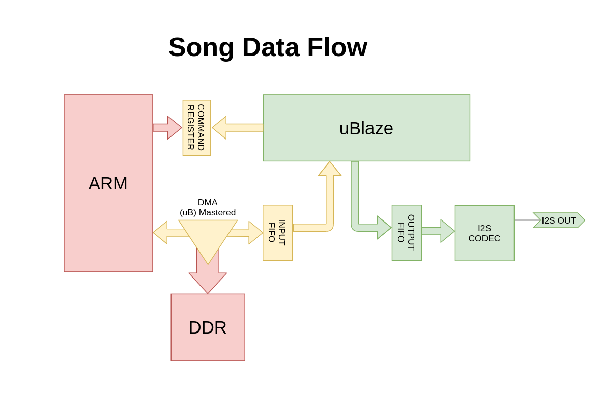
Several changes have been made to the MITRE reference design programmable logic to facilitate the implementation of an encryption scheme carried out by the microblaze. In the reference design, an AXI Direct Memory Access (DMA) module was used to transfer chunks of song to an FIFO. This fifo crosses from the main clock domain to the codec clock domain, and the I2S codec can pull samples from the FIFO at the designed sample rate, independent of the frequency of the main clock or the timing with which this FIFO is filled.
Our design introduces a new FIFO, hereafter termed the input FIFO, which becomes the new destination for the DMA. The output of this module connects directly to the microblaze via an AXI Streaming interface, a dedicated instruction in the microblaze allows a 32 bit read or write from this type of interface. Another streaming interface is used to write data to the original FIFO, now referred to as the output FIFO, which is connected to the codec. Our software need only treat these devices like pipes. Additionally, a GPIO module is provided to read the fill level of either FIFO.
The output FIFO's width has been changed to simplify connectivity, which requires samples to be written twice but enables future implementation of stereo audio capability with changes to software only. Also, the clock generation for the codec's clock domain can now be reconfigured by the microblaze, which would enable playback of audio with different sample rates with changes to software only.
	MSB                                                              LSB
[   UNUSED    (W)][   COMMAND   (W)][           STATUS          (R)]
W: write only, reads will return zero
R: read only, writes will have no effect
Commands from the miPod application are now issued through a shared register which generates an interrupt on the microblaze when written. The application side of the register cannot modify any commands it has already issued, and a new interrupt shall not be dispatched until it is acknowledged by a special write issued by the microblaze. This command register is also the means by which a hardware watchdog timer is reset.
# Watchdog
The integrity-checking module served to protect against voltage and temperature attacks, but it in no way ensures that the DRM is properly operating in a timely manner. The watchdog timer’s purpose is thus to make sure that the DRM is still responsive within a short window of time. This prevents several attacks which slow or halt the MicroBlaze. Xilinx provides an AXI Timebase Watchdog module, which uses a dual-expiration architecture. This generates an interrupt and a state bit is changed in the status register. If the MicroBlaze fails to clear the state bit before the next timeout, the WDT generates a reset signal. Thus, if the DRM halts or lags beyond a reasonable time threshold, the PL will assume an attack is occurring and reset the MicroBlaze. This solution maps the watchdog timer registers into the address space of the MB and creates an AXI connection between the WDT and the interrupt controller. The DRM code then handles the interrupt by clearing the status bits in the WDT status register.
# Integrity Monitor

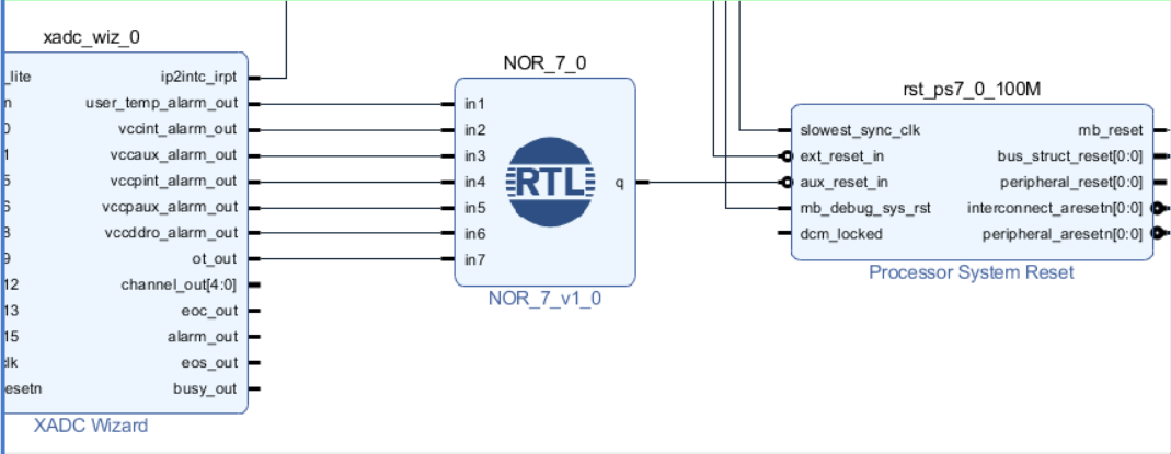
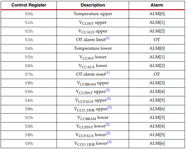
While less common, it is possible to retrieve or corrupt information by temperature attacks. Extreme cold temperatures can be used to halt a processor during operation, while extreme heat can result in errors and incorrect memory loading. Similarly, it has been demonstrated that tampering with voltages can cause errors to occur while a computer is processing secret information, resulting in a leak of secrets. To protect against these attacks, the FPGA has a built in ADC (XADC) that monitors temperature and voltage sensors. The module contains status registers which can be read either via JTAG or programmable logic. 7 alarm registers are also included as output signals which are active-HIGH. The alarms given, along with their respective status registers are shown in the figure below. Since the XADC also connects to the processing system via AXI, it is also possible to read the status registers from the processing system; however, it is better practice to read the status using the programmable logic. The solution arrived at was to combine the signals into an active-LOW reset signal using a 7-input NOR module whose output is tied to the proc_sys_reset module.

